New multicore STM32MP1 microprocessors (dual Cortex Ax + one Cortex Mx) with Linux OS for IoT applications (Cortex Ax) and real-time applications (Cortex Mx).
Now are available two macro STM32MP1 families that are:
Up to two A7 (@ 800 Mhz) + 3D GPU + M4 (@ 209 Mhz)
Up to two A7 (@ 650 Mhz) + 3D GPU + M4 (@ 209 Mhz)
- STM32MP1 introduction
- STM32MP1 user guide
- Getting Started with STM32MP1 Starter pack
- STM Presentations
- Flyer STM32MP1 Series Microprocessors
- Evaluation Boards
- STM32CubeMP1
- Important Links
- STPMIC1 – Power supply for STM32MP1 and in general for MPU
.
STM32MP1 introduction
The STM32MP1’s flexible architecture is ideal for Linux and real-time applications.
Its mainlined:
- OpenSTLinux Distribution
- STM32Cube ecosystem drastically reduce development time.
- Purchase Discovery kits or Evaluation boards for STM32MP1 microprocessors.
- Download the free STM32CubeMP1 embedded software package containing the HAL, LL (low-layer) APIs, and middleware. Then install ST’s STM32CubeMX graphical software configuration tool (free) that supports pinout configuration, code generation and a power consumption calculator. Start with one of the many examples provided or build your own project.
- STM32MP1 users can now choose from several IDEs from leading vendors and enjoy free license
Learn more about our microprocessor solution on wiki, community or blog article.
The first group of STM32MP1 microprocessor series comes with dual Arm® Cortex®-A7 and Cortex®-M4 Cores
A general-purpose microprocessor portfolio enabling easy development for a broad range of applications, the STM32MP1 series is based on a heterogeneous single or dual Arm Cortex-A7 and Cortex-M4 cores architecture, strengthening its ability to support multiple and flexible applications, achieving the best performance and power figures at any time.
The Cortex-A7 core provides access to open-source operating systems (Linux/Android) while the Cortex-M4 core leverages the STM32 MCU ecosystem.
.
The STM32MP1 comes with many benefits including a rich development ecosystem:
- Mainlined open-source Linux distribution with Android support available via partners
- STM32Cube firmware and embedded software libraries for Cortex-M4 core
- An optional 3D graphics processing unit (GPU) provides for advanced HMI development
- Rich set of digital and analog peripherals
- Advanced security features
- Optimized bill of materials (BOM) thanks to: High integration, packages compatible with low-cost PCB technologies (down to 4-layer plated-through hole (PTH) PCBs) and dedicated Power Management IC (PMIC)
- Advanced tools from ST and Partners
- Best-in-class local and online support
- An extensive third-party ecosystem is available to help developers thanks to the ST Partner Program.
- Rolling 10-year longevity commitment renewed every year
.
Flexible architecture
The single or dual Cortex-A7 cores are dedicated to open-source operating systems while the Cortex-M4 core is dedicated to real-time and low-power tasks.
- Dual Cortex®–A7 cores running at 650 MHz
- 32-Kbyte L1 Instruction cache
- 32-Kbyte L1 Data cache
- 256-Kbyte Level 2 cache
- Cortex®–M4 core running at 209 MHz
- a single-precision floating point unit (FPU)
- a full set of digital signal processor (DSP) instructions
- memory protection unit for enhanced application security
The Cortex-M4 core benefits from an embedded SRAM (448 Kbytes) to run purely deterministic code.
For instance, a customer currently using an STM32 MCU based on STM32Cube firmware, could transparently fully re-use his code on the Cortex-M4 core’s 448 Kbytes of SRAM, and add the Linux application (for instance an HMI) running on the Cortex-A7 core(s).
To meet a broad range of applications requirements, most peripherals can be allocated to either the Cortex-A7 or Cortex-M4 cores.
.
Power efficiency
- Dynamic efficiency: the Cortex-A7 and Cortex-M4 cores can be run or stopped independently to achieve the best power efficiency for each processing and real-time application requirement.
- Low-power modes: Multiple low-power modes are available including:
- Standby mode: Down to 36 µW.
- VBAT mode: Down to 4.5 µW. In this mode, it is possible to keep track of time using the real-time clock while keeping the system secure thanks to the tamper detect feature.
.
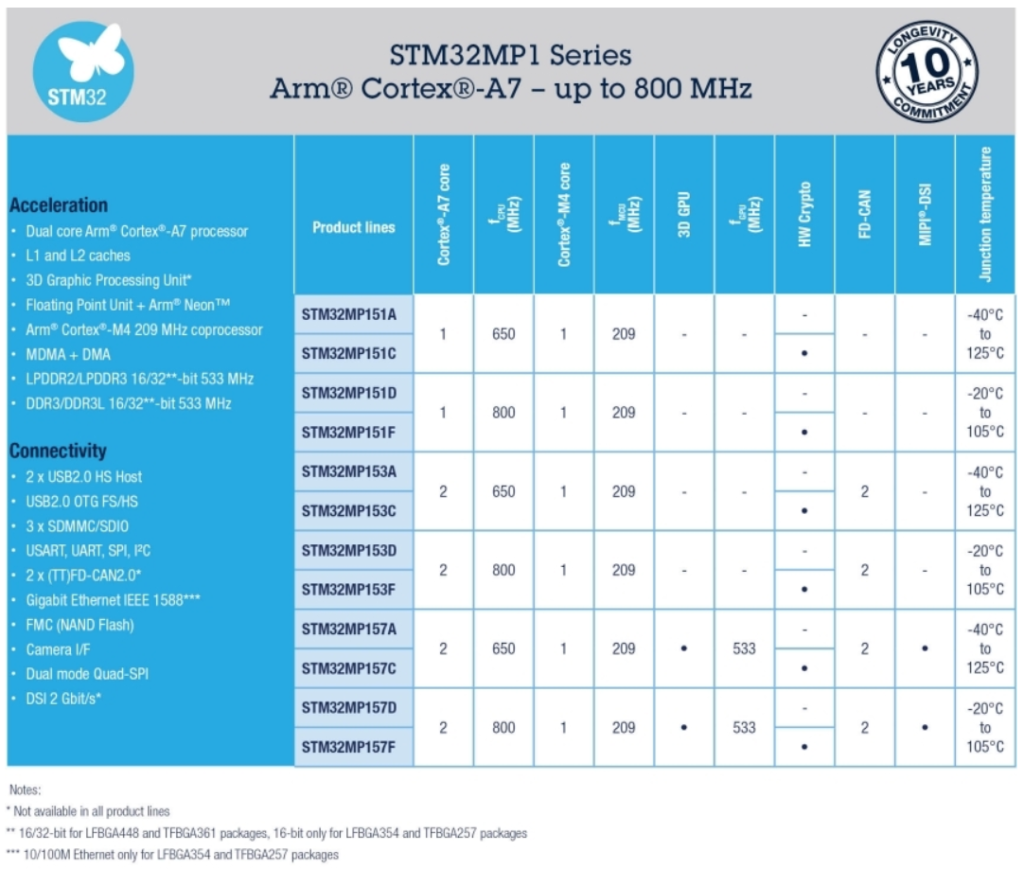
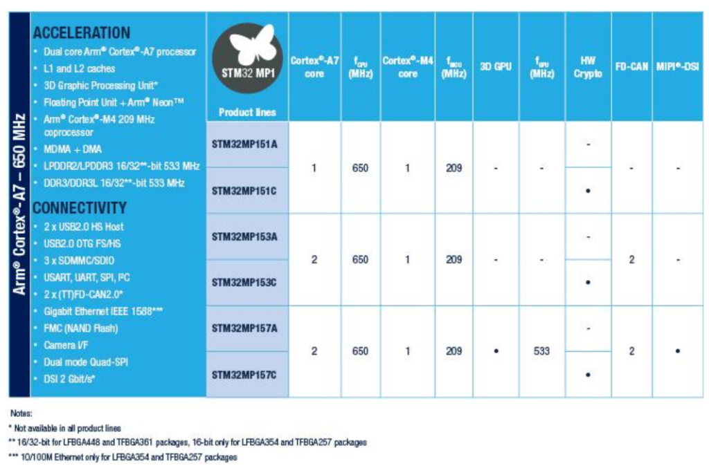
The STM32MP1 series is available in 3 different lines which are pin-to-pin compatible:
- STM32MP157: Dual Cortex-A7 cores @ 650 MHz, Cortex-M4 core @ 209 MHz, 3D GPU, DSI display interface and CAN FD
- STM32MP153: Dual Cortex-A7 cores @ 650 MHz, Cortex-M4 core @ 209 MHz and CAN FD
- STM32MP151: Single Cortex-A7 core @ 650 MHz, Cortex-M4 core @ 209 MHz
Each line comes with a security option (cryptography & secure boot)
.
Evaluation Boards
- STM32MP157A-DK1 – Discovery kit with STM32MP157A MPU
- STM32MP157A-EV1 – Evaluation board with STM32MP157A MPU
- STM32MP157C-DK2 – Discovery kit with STM32MP157C MPU
- STM32MP157C-EV1 – Evaluation board with STM32MP157C MPU
.
STM32CubeMP1
STM32CubeMP1 is for STM32MP1 series (HAL, Low-Layer APIs and CMSIS (CORE, DSP, RTOS), OpenAMP for Inter processor communication.
Coming with examples running on ST boards: Discovery kits (DK) and Evaluation boards (EV).
.
Important Links (wiki)
- The wiki is user manual of the STM32MPU Embedded Software distribution, see here.
- New release STM32MP15-Ecosystem-v1.1.0
- Including :
- V1.1.0 Distribution for Android 9 Support
- CubeIDE V1.1.0 to support Cortex M4 Co-processor
- GitHub – STM32MPU_EmbSW_Android_Overall_Offer
- Including :
- Wiki, Getting started
- Wiki, Development Zone
- Wiki, Release notes
- Wiki, Which Package better suits your needs
- Wiki, Embedded software
- Wiki, OpenSTLinux distribution
- Wiki, STM32CubeMP1 Package
- Wiki, Embedded software components
- Wiki, Linux Operating System
- Wiki, I2C overview
- Wiki, ALSA overview
- Wiki, DRM KMS overview
- Wiki, Wayland Weston overview
- Wiki, Trace and debug tools
- Wiki, Trace and debug overview per Linux software frameworks
- STM32MPx partner
- OpenSTLinux licenses
- STM32MP1 Series system power consumption (AN5284)
- The GNU General License
.
STPMIC1
STPMIC1 – power supply for STM32MP1 and in general for MPU
The STPMIC1 is a fully integrated power management IC designed for products based on high integrated application processor designs requiring low power and high efficiency.
The device integrates advanced low power features controlled by a host processor via I²C and IO interface.
The STPMIC1 regulators are designed to supply power to the application processor as well as to the external system peripherals such as: DDR, Flash memories and other system devices.
The boost converter can power up to 3 USB ports (two 500 mA host USB and one 100 mA USB OTG).
Its advanced bypass architecture allows the smooth regulation of VBUS for USB ports from a battery as well as low-cost consumer 5 V AC-DC adapters.
4 buck SMPS are optimized to provide an excellent transient response and an output voltage precision for a wide range of operating conditions, high full range efficiency (η up to 90%) by implementing a low power mode with a smooth transition from PFM to PWM and also an advanced PWM synchronization technique with an integrated PLL for a better noise (EMI performance).
Key Feature
* Input voltage range from 2.8 V to 5.5 V
* 4 adjustable general purpose LDOs
* 1 LDO for DDR3 termination (sink-source), bypass mode for low power DDR or as general purpose LDO
* 1 LDO for USB PHY supply with automatic power source detection
* 1 reference voltage LDO for DDR memory
* 4 adjustable adaptive constant on-time (COT) buck SMPS converters
* 5.2 V / 1.1 A boost SMPS with bypass mode for 5 V input or battery input
* 1 power switch 500 mA USB OTG compliant
* 1 power switch 500 mA/1000 mA general purpose
* User programmable non-volatile memory (NVM), enabling scalability to support a wide range of applications
* I²C and digital IO control interface
* WFQFN 44L (5x6x0.8)
Up to now are available three model that are:
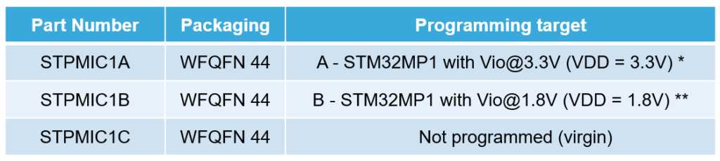
* Typical application: 5V wall adapter powered application
** Typical application: Li-Ion/Li-Po battery powered application